The HP 70621A module provides a low-noise, high-gain amplification stage that can be used in front of an RF section in HP70K systems. The 70621A provides amplification of signals from 100 kHz to 2.9 GHz, and is typically used in conjunction with a 70904A module. By adding pre-amplification, system noise can be reduced by 6–11 dB, and sensitivity can be improved by approximately 20 dB. Pre-amplification can also be used after, before, or both before and after a pre-selector.
The 70621A also provides a 28 VDC output to power an RF noise source. When a noise source is coupled with the 70621A, the bandpass/rejection characteristics of filters and the linearity of amplifiers can be easily tested without requiring a tracking generator.
Using an integrated preamplifier has several advantages when compared to external signal processing. The 70621A automatically calibrates measurement units displayed on-screen, corrects for gain and flatness, adjusts IF gains as needed, and adjusts RF attenuation to ensure that maximum mixer levels are not exceeded.
Inside the 70621A

The major components visible on this side are, from left to right:
K1 — Transfer Switch Assembly
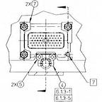
A5 — RF Amplifier Assembly
A closeup of the RF Amplifier Assembly is shown below:

The RF INPUT from the front panel is routed to the Transfer Switch Assembly (K1), which allows the amplifier to be bypassed. When not bypassed, the signal is routed through a frequency limiter, which ensures that signals above 3 GHz are not passed, then through the RF Amplifier Assembly (A5). The output of the RF Amplifier Assembly (A5) is then routed back through the Transfer Switch Assembly (K1), to the RF OUTPUT on the front panel.

The major components visible on this side are:
A2 — Controller/Power Supply Board Assembly.
This board controls the bypass switch, generates and switches the 28 VDC for an external noise source, and generates voltages required for the amplifier.
The block diagram of the 70621A is:

Here we can see the switch drivers and noise source drivers, and how the Transfer Switch Assembly (K1) switches the RF Amplifier Assembly (A5) in and out of the circuit.
Inside the 70621A OPT H50

Option H50 replaces K1 with two separate microwave switches, eliminates the noise source output, and adds provisions for an external notch filter before the amplifier input.
The RF INPUT from the front panel is routed to the first transfer switch, which routes it to a front panel SIGNAL OUTPUT or to the rear panel EXT NOTCH FILTER OUTPUT connector. The rear panel EXT NOTCH FILTER INPUT connector is routed through RF Amplifier Assembly (A5) to the second transfer switch. The front panel RF OUTPUT is then switched between the amplifier output or the front panel SIGNAL INPUT connector.
If the front panel SIGNAL INPUT and SIGNAL OUTPUT connectors are connected together, this effectively allows the amplifier to be bypassed. If the two rear panel connectors are also connected using a 3GHz frequency limiter, the Option H50 70621A is functionally equivilent to a stock 70621A.
Interesting Experiments
Typically, the 70621A is configured as a slave module under the 70900A or 70900B. It would be interesting to test to see if the module is usable when configured as a master, and if amplification and/or the noise source voltage output can be independently controlled.
The 70621A also provides a good starting point for building semi-custom amplification, filtering and RF processing subsystems. However, this will only be useful if the module can run independently from the spectrum analyzer, otherwise the offsets and corrections will result in incorrect results.
Module Resources
Installation and Verification Manual:
Service Manual: